
Our laboratory is equipped with experimental facilities dedicated to the elaboration of nanostructures as well as to their optical characterization. For any supplemental information about these facilities, please contact the responsible, Eloïse Devaux (devaux@unistra.fr)
Sample preparation
- Chemistry room equipped with facilities for substrates cleaning and samples preparation (sonicator, oven, ozone cleaner, spin-coater, etc…)
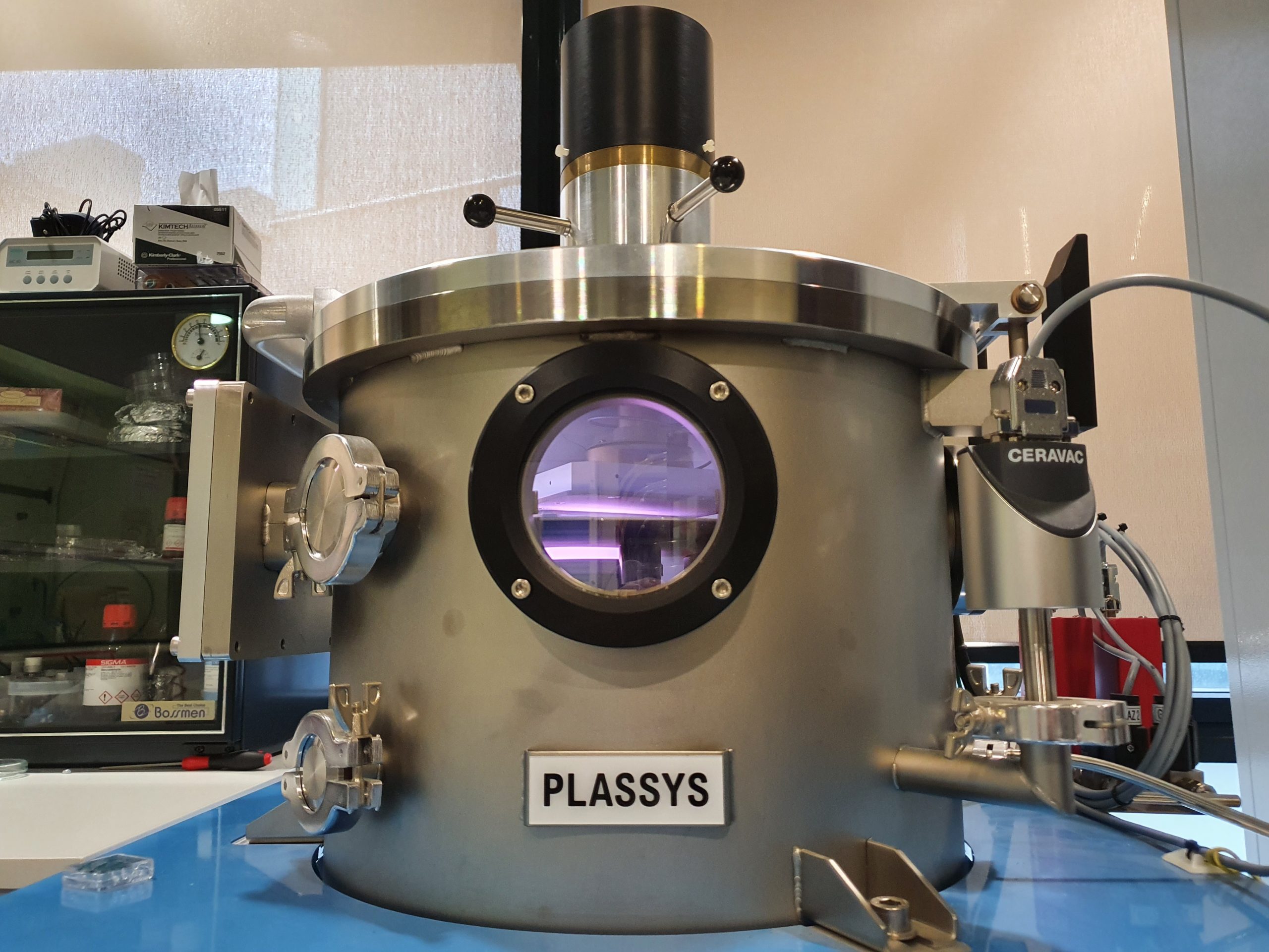
- Egun evaporator Plassys (ME300) with four crucibles (generally loaded with Au, Ag, Cr and Al). Heating system on the substrate holder ( for a 3″ diameter substrate or four 2″ susbstrates)
- Metal magnetron sputterer Plassys (MP300) with two targets (generally Ag and Al). Cooling system on the susbrate holder (for a single 2″ substrate)
- Dielectric RF sputterer Plassys (MS300) with two targets (generally SiO2, Al2O3, Si, TiO2, etc… ) (for a single 2″ substrate)
- Metal magnetron “table-top” sputterer Safematic (CCU-010) with one target (generally Au or Ag) (planetary/rotatory stage)
For characterization of the morphology of the samples, we have access to a profilmeter and an AFM in Samori’s group, and to the SEM of the institute (Quanta FEG 250 from Thermofischer company, equipped with EDX and working in ESEM). But we have also our own FIB/SEM system described here below.
Sample fabrication
We have our own FIB/SEM system (Focused Ion Beam and Scanning Electron Microscope). It is a cross-beam Auriga from Zeiss company (acquired in 2013). FIB allows the direct milling of any material with a high resolution (below 10nm), as well as the ion-induced deposition/etching of materials. SEM, in addition to be a powerful tool for sample characterization, allow us to extend our toolbox for doing nanostructures by e-beam lithography. In addition, the system is fully equipped with options allowing a wide range of tasks :
- Single GIS (Gas Injection System) for Pt deposition
- Multi-GIS for Au,W,SiOx deposition and XeF2 and Water for gas assisted etching of respectively Si based and Carbon based materials
- EDX detector for qualitative and semi-quantitative analysis
- BSD detector for collection of back-scattered electrons for analysis
- Charge-compensation system to do SEM imaging of non-conductive materials
- Flood Gun to do FIB milling of non-conductive materials
- Fast Beam Blanker for e-beam lithography
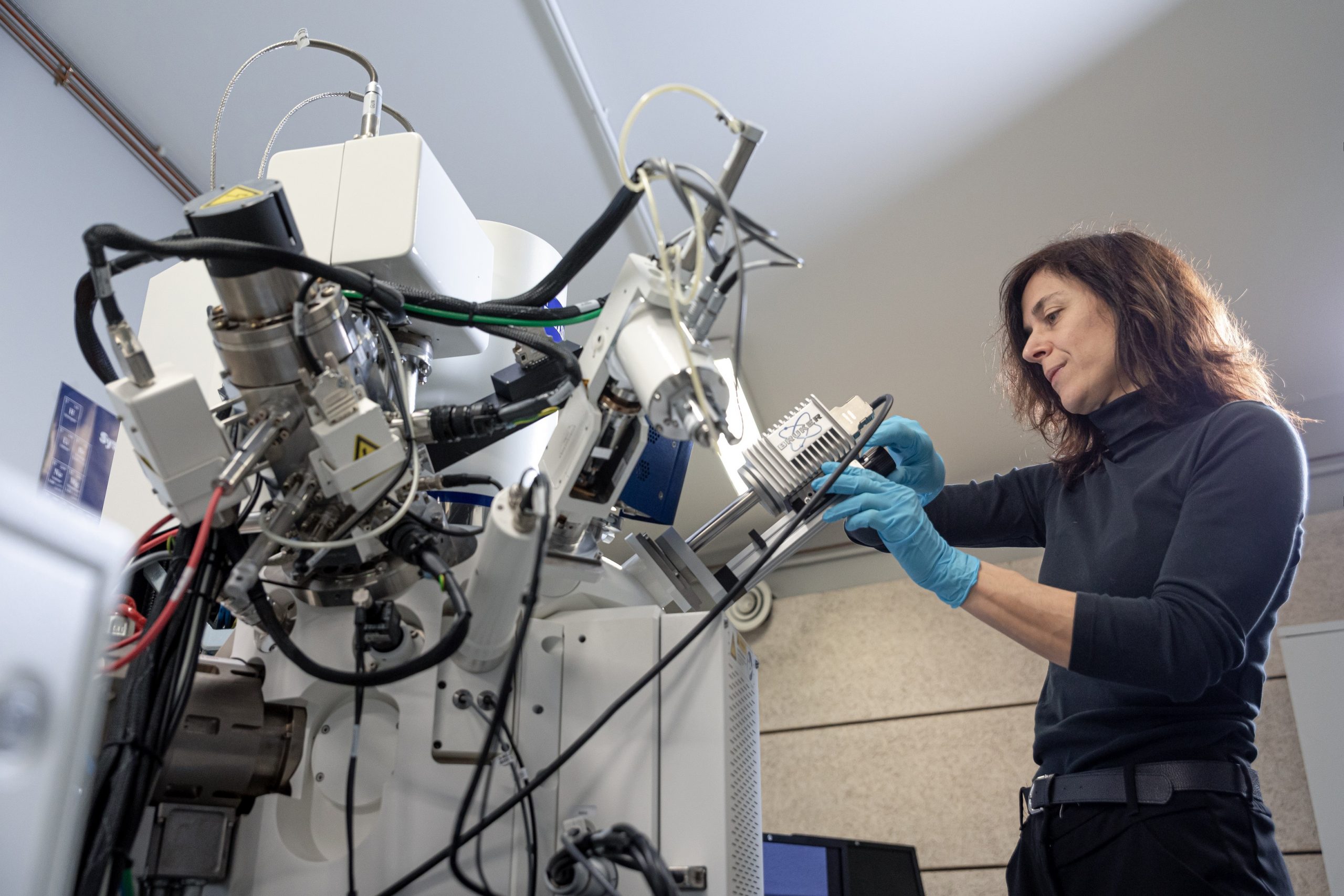
Photo : FRC
But for those who are more micro than nano, we have also access to the Laser Writer of Samori’s group, or to the mask aligner of ISIS, located in the clean room, allowing to create structures from 1µm to many mm size.
Optical characterization
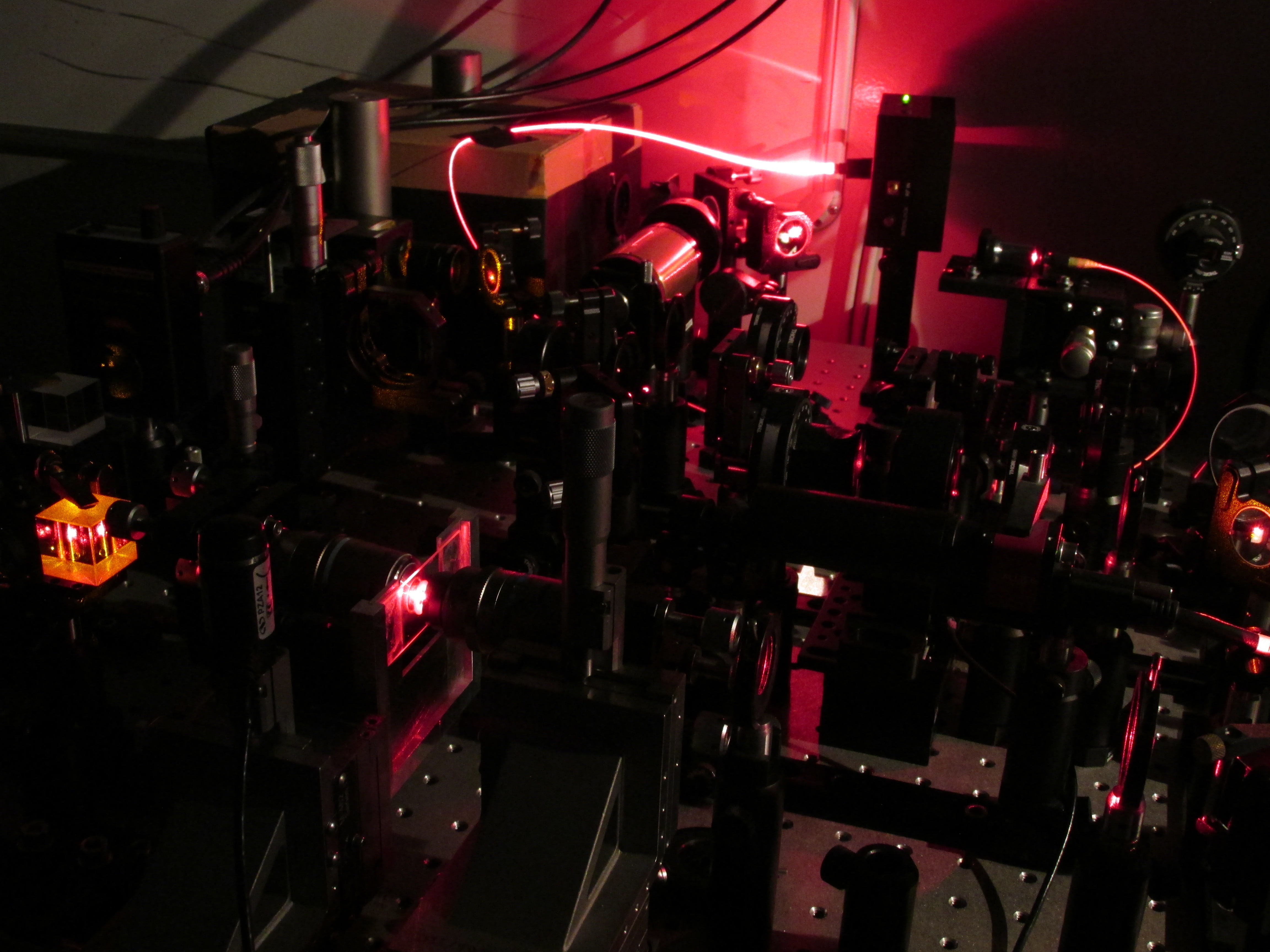
We have different spectrometers covering the whole optical range from UV to far-IR, some microscopes, many lasers sources and cameras with different optical setups, etc… Here is a non-exhaustive list, please contact us for more details :
- Spectrophotometer ARC spectra Pro 300i mounted on an inverted microscope Nikon Eclipse TE200 (UV-visible)
- Spectrophotometer Shimadzu UV3101PC (UV-visible-NIR)
- Spectrophotometer Shimadzu UV2600 (185-900nm)
- Spectrofluorometer Jobin-Yvon Fluorolog
- Spectro Bruker Vertex 70 FTIR (mid IR)
- Spectro Bruker Invenio (far to mid-IR)
- Hamamatsu Quantaurus C11347 quantum yield spectrometer
- Confocal microscope Nikon
- Spectra Physics Spitfire femtosecond laser equipped with an HELIOS Transient Absorption Spectrometer.
- Supercontinuum laser NKT
- Home made optical setups (Optical traps, Mueller polarimetry in visible)
- Flash photolysis LP980 Edinburgh Instruments (fully automated system for acquiring transient absorption kinetics and spectra based on the laser flash photolysis technique)
Miscelleanous
- 4- Probe station for conductivity measurements
- Autolab potentiostat/galvanostat for electrochemistry (now in Giulio Ragazzon group)